
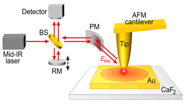
Chengdu Miji Technology Co., Ltd. successfully delivered a terahertz near-field optical microscopy system to Henan University of Technology in 2024. This system can perform reflection-mode terahertz near-field imaging. The system mainly consists of a solid-state source (97.8 GHz, 80 mW), a detector, and a dedicated near-field atomic force microscope main unit.
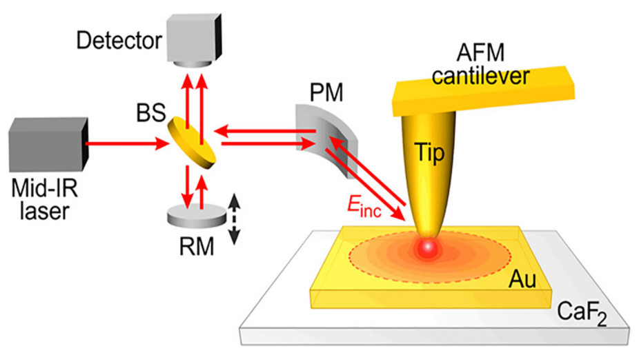
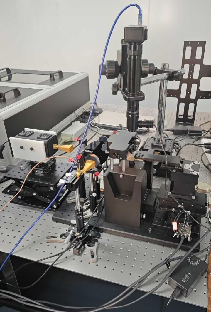
System functions:
The system is a scattering-type terahertz near-field scanning imaging system, consisting of an AFM optimized for scattering near-field, a sample scanner with XY closed-loop and Z open-loop scanners, and integrated parabolic mirrors including a three-dimensional motorized stage to focus external light onto the AFM tip. The system can effectively extract near-field signals and suppress background noise: it supports simultaneous signal demodulation per pixel for the 1st to 3rd harmonic orders of the tip frequency for two independent signals (mechanical/AFM and s-SNOM signals).
Terahertz near-field imaging:
Terahertz near-field microscopy is a technique that uses terahertz waves (frequency range approximately 0.1–10 THz, wavelengths from 30 μm to 3 mm) for high-resolution imaging. Traditional terahertz imaging is limited by the optical diffraction limit, with its resolution typically comparable to the wavelength. However, by exploiting the tip-enhanced effect, THz s-SNOM can overcome this limit, confine terahertz waves to nanoscale volumes, realize nanoscale super-resolution imaging while preserving the unique spectral characteristics of the terahertz band, and effectively enhance weak terahertz signals through surface plasmons, tip-field enhancement, and resonant structures. This technology holds important application prospects in fields such as materials science, biomedicine, physical chemistry, and semiconductor inspection.
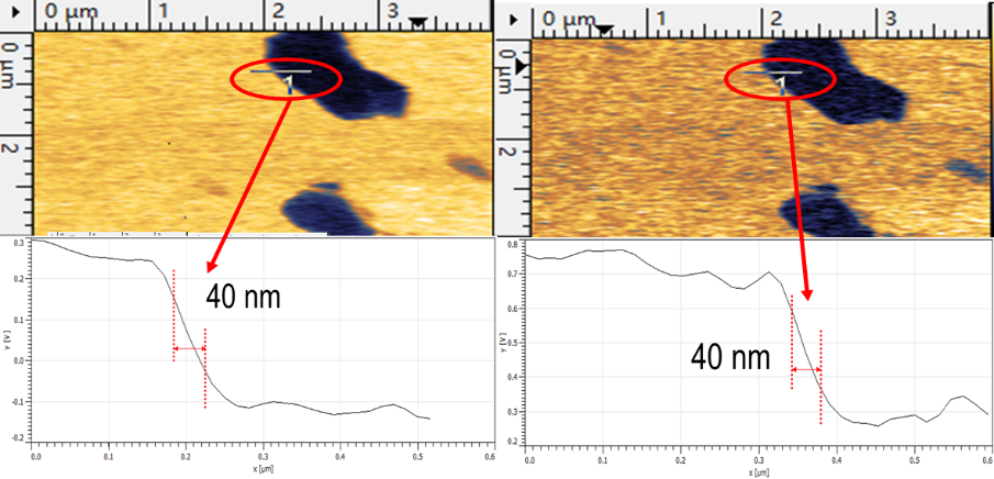
The terahertz scattering-type near-field imaging system launched by Miji Technology adopts a high signal-to-noise ratio terahertz system, capable of up to 3rd-order near-field imaging, and simultaneously acquires AFM topography data of the sample surface. Actual measurements show that the system can achieve nanoscale resolution
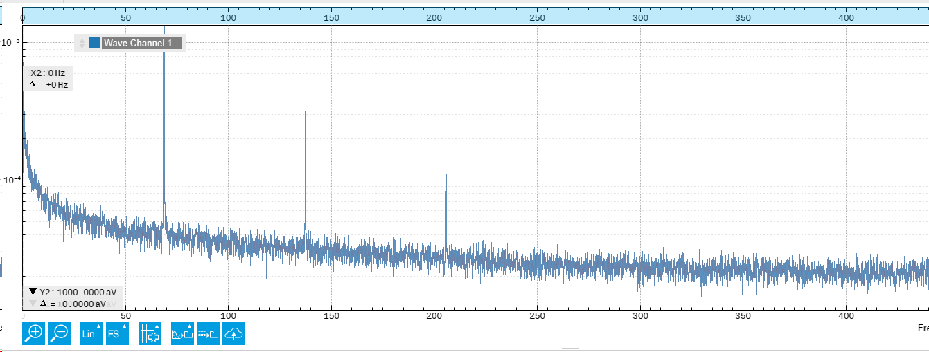
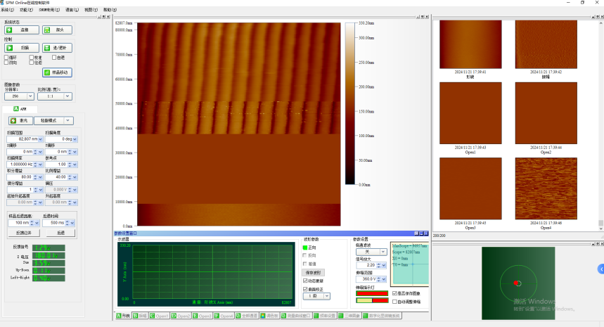
While pursuing near-field imaging quality, the system also provides maximum user-friendliness in software: a workflow-based system operation user interface that is clean and simple, allowing researchers or staff who are not yet familiar with near-field imaging to get started easily in a short time.
The atomic force microscope (AFM) in the near-field system adopts an open architecture, specially designed for near-field optical applications. Unlike most conventional AFMs on the market, near-field optical AFMs need to maintain spatial openness while possessing multi-channel demodulation output capability. The open architecture design ensures that external light sources (such as visible light, infrared light, and terahertz waves) can be precisely focused onto the tip position. Currently, mainstream near-field AFM equipment on the market is mainly from German brands (e.g., Nearspec series and Bruker IR series). Although they offer excellent performance, they are expensive and difficult to integrate efficiently with customers’ own terahertz systems. In response to this situation, our company’s developed near-field AFM, while maintaining an open architecture, designs various types and focal lengths of custom off-axis focusing mirrors, which can more widely adapt to various types of terahertz sources, significantly enhancing the equipment’s compatibility and practicality.
Source: Chengdu Miji Technology Co., Ltd. official website View original text